Yield Engineering Systems opens new advanced technology center in Arizona to support semiconductor growth in the U.S.
Yield Engineering Systems opens new advanced technology center ... City of Chandler (.gov)

Yield Engineering Systems Opens New Facility in Chandler, Arizona
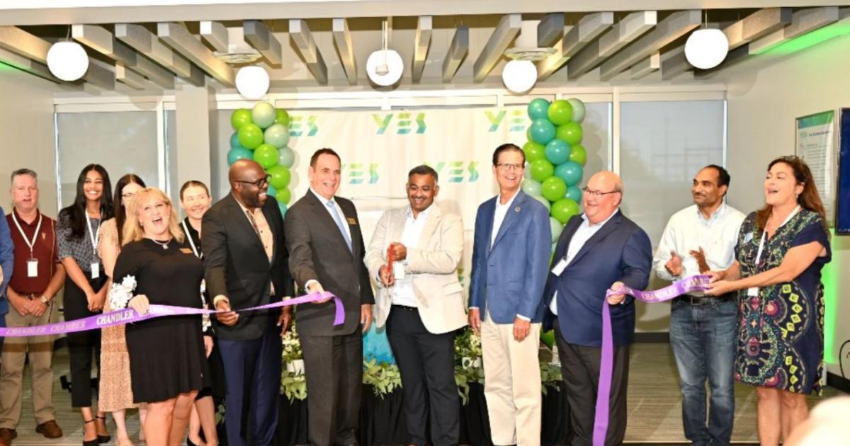
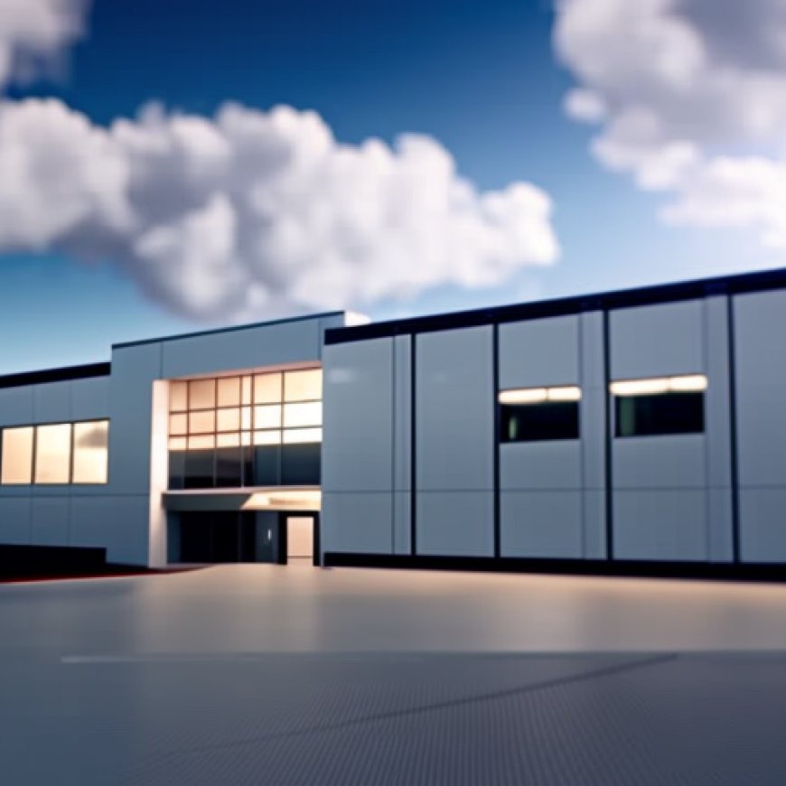
CHANDLER, Ariz. – Yield Engineering Systems (YES), a leading provider of technology solutions and process equipment for the semiconductor ecosystem and applications, held a ribbon-cutting ceremony today for its new 123,000-square-foot facility in Chandler, Arizona. The facility is located at 3200 W. Germann Road within the Price Corridor employment center.
The YES Advanced Technology Center (YATC)
The state-of-the-art YES Advanced Technology Center (YATC) will include 50,000-square-feet of manufacturing space for unparalleled semiconductor manufacturing and process development. There will also be a 10,000 square foot cleanroom in the first development phase that will be expanded to approximately 40,000 square feet in the future. The cleanroom will allow YES to collaborate with its customers to develop innovative processes and validate platform prototypes.
Commitment to Sustainable Development Goals
For over four decades, YES has been at the forefront of research and development that has pioneered new equipment used in semiconductor fabs throughout the world. Its portfolio encompasses cutting-edge technology and innovative hardware that drives advancements in multiple industries, from artificial intelligence and high-performance computing, to life sciences and mixed reality applications.
“YES has been financially supported by KCK Group for the past six years,” said Krishna Nety, Board Member of YES and Senior Managing Director at KCK Group. “YES’s continued growth and success is an excellent example of KCK’s commitment to American competitiveness, driven by industrial and emerging technologies.”
“YATC not only provides our customers and partners with state-of-the-art equipment for novel process development, but it is also a center that will bring best-in-class manufacturing of complex products in collaboration with our supply chain partners with an innovative business model, that enables significant job creation in the United States,” said Rama Alapati, CEO of YES. “We are thankful and proud to partner with the City of Chandler, State of Arizona and the federal government in bringing the YATC to life.”
Rezwan Lateef, President of YES added, “Designed to the highest standards of safety and workplace efficiency, the YATC will play a central role in our R&D collaborations with our global customer base and help them execute their exciting technology roadmaps. It also reflects our commitment to the United States’ effort to build a strong domestic semiconductor industry, and we are proud to be a part of Arizona’s burgeoning technology ecosystem.”
Investment in Sustainable Semiconductor Manufacturing
Supporting the rapid expansion of the American semiconductor manufacturing infrastructure, YES has invested $25 million in the facility and aims to use it as a center of excellence that will help strengthen the semiconductor industry in Arizona and the entire US-based semiconductor ecosystem. The YATC should be complete by the end of 2023 and employ approximately 100 people, further propelling the region’s technological prowess.
Government Officials and Community Stakeholders
Several prominent government officials and community stakeholders also commented on the new YATC facility:
- Arizona Senior Senator Kyrsten Sinema, Chair of the Senate Space and Science Subcommittee, stated, “Yield Engineering System’s new YATC facility will strengthen Arizona’s leadership as a hub for semiconductor manufacturing. That’s why I was proud to help pass our bipartisan CHIPS and Science Act into law to fuel Arizona careers, keep Americans safe against foreign adversaries like China, and boost our economic competitiveness.”
- Rep. Greg Stanton stated, “The East Valley is metro Phoenix’s hub for advanced manufacturing, and we didn’t develop that reputation by accident. It’s thanks to years of hard work, planning and targeted investments like our bipartisan CHIPS Act. I couldn’t be more excited that leading companies like YES have chosen to take advantage of all that Chandler has to offer and expand their operations to meet the growing demand.”
- Sandra Watson, President and CEO of the Arizona Commerce Authority, stated, “We are excited to celebrate Yield Engineering Systems’ Technology Center grand opening in Chandler. With a focus on manufacturing excellence and innovative research and development operations, YES’s new facility is a valued addition to Arizona’s growing semiconductor industry.”
- Chris Camacho, President and CEO of the Greater Phoenix Economic Council, stated, “The inclusion of Yield Engineering Systems into our ecosystem presents another arm to our dynamic industry. With its manufacturing capabilities and commitment to collaboration on new, innovative processes, YES will grow as a key piece of the Chandler and Greater Phoenix semiconductor ecosystem.”
- Chandler Mayor Kevin Hartke, stated, “We are thrilled to officially welcome another high-value semiconductor supplier with the addition of Yield Engineering Systems. Chandler’s exceptional workforce and business-friendly environment continue to put our community on the short list for these highly competitive projects. We appreciate the significant investment that YES is making in Chandler and the new job opportunities that will be available in our community.”
Contact Information
- Stephanie Quinn
Kiterocket, on behalf of YES
squinn@kiterocket.com - Alyssa Tufts
Arizona Commerce Authority, Public Relations Director
alyssat@azcommerce.com
602-845-1243 - Stephanie Romero
City of Chandler, Public Information Officer
stephanie.romero@chandleraz.gov
480-782-2231
About YES
Yield Engineering Systems (YES) is a provider of surface and materials enhancement technology solutions. YES’ high-tech process equipment helps bring to life complex processes that enable artificial intelligence (AI), high performance computing (HPC), sciences and mixed reality applications. YES’ highly advanced thermal processing systems, deposition systems, and wet etch and clean technologies play a vital role in the processing of advanced node silicon wafers, next-generation substrates, wafer- and panel-level packages, power semiconductors, life compound semiconductors, internet of things (IoT) devices, microLED and miniLED displays, and micro-fluidic consumables for genomics. With innovative technologies designed to optimize performance and cost of ownership, YES serves as a trusted partner from startups to Fortune 100 companies in a wide range of markets. YES is headquartered in Fremont, California. To learn more about YES’ systems and service offerings, visit Yield Engineering
SDGs, Targets, and Indicators
1. Which SDGs are addressed or connected to the issues highlighted in the article?
- SDG 9: Industry, Innovation, and Infrastructure
- SDG 8: Decent Work and Economic Growth
2. What specific targets under those SDGs can be identified based on the article’s content?
- SDG 9.2: Promote inclusive and sustainable industrialization and foster innovation
- SDG 8.5: By 2030, achieve full and productive employment and decent work for all women and men, including for young people and persons with disabilities, and equal pay for work of equal value
3. Are there any indicators mentioned or implied in the article that can be used to measure progress towards the identified targets?
- Investment in a new facility (123,000-square-foot) for semiconductor manufacturing and process development
- Creation of a cleanroom for collaboration with customers to develop innovative processes and validate platform prototypes
- Investment of $25 million in the facility
- Employment of approximately 100 people
4. Table: SDGs, Targets, and Indicators
| SDGs | Targets | Indicators |
|---|---|---|
| SDG 9: Industry, Innovation, and Infrastructure | SDG 9.2: Promote inclusive and sustainable industrialization and foster innovation | – Investment in a new facility (123,000-square-foot) for semiconductor manufacturing and process development – Creation of a cleanroom for collaboration with customers to develop innovative processes and validate platform prototypes |
| SDG 8: Decent Work and Economic Growth | SDG 8.5: By 2030, achieve full and productive employment and decent work for all women and men, including for young people and persons with disabilities, and equal pay for work of equal value | – Investment of $25 million in the facility – Employment of approximately 100 people |
Behold! This splendid article springs forth from the wellspring of knowledge, shaped by a wondrous proprietary AI technology that delved into a vast ocean of data, illuminating the path towards the Sustainable Development Goals. Remember that all rights are reserved by SDG Investors LLC, empowering us to champion progress together.
Source: chandleraz.gov
![]()
Join us, as fellow seekers of change, on a transformative journey at https://sdgtalks.ai/welcome, where you can become a member and actively contribute to shaping a brighter future.